Reduced-Temperature Synthesis of Large-Area, Monolayer Graphene
A major challenge to fully realize the potential of graphene-based technologies is to reproducibly fabricate large-area high-quality graphene. We have recenlty shown a new method that employs plasma-assisted chemical vapor deposition (CVD) techniques for producing highquality large-area (~ 1 cm2) monolayer graphene on copper at reduced temperature (RT) . The properties of this graphene are found to be superior to conventional, thermally grown graphene.
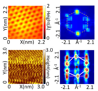
RT-Graphene Comparison of the representative microscopic structures of graphene grown at different temperatures and on copper: From left to right, surface topographies of graphene taken at 77 K and the Fourier transformation (FT) of large-area topography (second column), for top row, RT-grown on Cu foil and (bottom row) 1000 C-grown on Cu foil. The morphology of the graphene grown at high temperature is distorted by thermal mismatch stress unlike RT graphene.
Plasmon Heating
At the nanoscale both the optical and thermal transport properties of nanostructures are much different than even the microscale. Certain metal nanoparticles have strong intereactions with visible light due to an electron resonane effect known as a plasmon resoance. At the resonant frequency, light is strongly absorbed and this energy is converted to heat in tens of nanoseconds. For nanoparticles on a substrate, the transfer of heat from the particle is reduced as the size of particle is smaller than the phonon mean-free path of the substrate. This makes it is possible to locally heat metal nanoparticles to very high tempereatures with low intensity laser.
Plasmon Assisted Chemical Vapor Deposition
Heat is necessary for many physical, biological, and chemical processes. For example, chemical vapor deposition (CVD), which is a widely used method for material deposition, involves exposing a heated substrate to vaporized chemical precursors that react and deposit material. Typically, the entire process takes place inside an oven, but if the heat could be localized, so could the deposition.
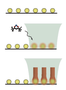
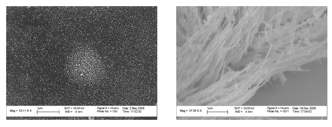
Plasmon Assited Chemical Vapor Deposition If excited nanopartlcies are in CVD. environment, material deposition can be localized. Consider an array of nanoparticles on suface, shown in the top left illustration (top to bottom). An array of noparticles is placed in a CVD environment. A focused laser heats the nanoparticles. Deposition occurs on the nanoparticles. We referr to this method as Plasmon Asssited CVD (PACVD) Shown in the schematic are SEM image of PACVD of PbO.
Plasmon Optofluidics--Using Light to Manipulate Fluids
Bubble assisted interphase-mass transfer (BAIM) (a) An array of metal nanoparticles is incorporated in the base of microfluidic channel (top). A laser near the resonant frequency of the nanoparticle array is focused on the substrate, heating the particles. The heat from the nanoparticles is transferred to the surrounding fluid resulting in evaporation into the gas bubble and subsequent mass-transfer to the opposite side of the bubble. Applications include: (b) pumping fluid along a microchannel (left to right) starting at top, and (c) preconcentration of delicate molecules: before, top, and after BAIM, (bright). The local concentration of DNA oligomers increases by a factor of 5X in 10 min.
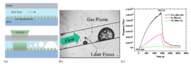
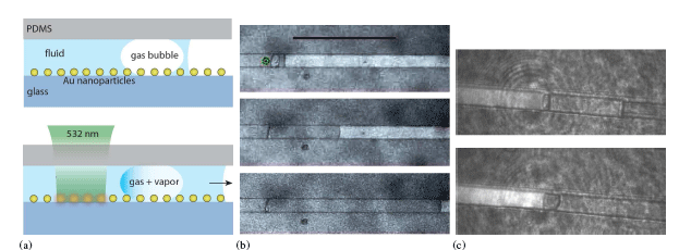
Micro-Chemical Reactor. a) Schematic of the process (side view). A microfluidic channel with gold nanoparticles attached to the base; fluid flows from left to right. (Top) A laser at or near the frequency of the plasmon resonance of the gold nanoparticles is focused on the substrate, and the subsequent heat generated in the nanoparticles is transferred to the surrounding fluid and forms vapor. The vapor phase components reacts on the catalyst forming gas bubbles which are carried downstream. (The channel height is 40 um and the radii of the nanoparticle is ~ 10 nm. b) Image (video) of the microchannel taken during the process (top view). . The fluid is 1:1 ethanol and water. A gas plume can be seen emanating from the laser spot and forming bubbles. c) The partial pressure with time of CO2 (M/z=44), H2 (M/z=2), and CO (M/z=12), as measured by RGA. Time =0 s is when the PAC process starts, and it ends at t = 1500 s.
Nanoscale Architecture: Synthesis
Architecturally engineered nanoscale materials present opportunities for advancing existing and developing new synthesis methods. Of particular interest are techniques that provide a high degree control of particle size uniformity and inter-particle spacing, and are scalable to large areas. Block copolymer lithography (BCPL) is an emerging, self-assembly technique that allows for creation of highly uniform, ordered arrays of nanoparticles on planar and non-planar surfaces alike. The structures can be engineered, for example, changes in the solvent chemistry give rise to more complex structures: Ni anoprints" b; and three dimensional inverse-opal structures of rhodium oxide, Figure c. Potentially, BCPL could be used to create arrays of catalysts, ordered mixtures of catalysts, and more advanced structures such as ordered arrays of rods, which could allow for strong optical coupling. BCPL is low-cost and scalable to large areas, and I believe will have many applications in energy conversions including solid-oxide fuel cell catalysts, photovoltaic photo-sensitizers, and advanced PACT devices. We have recently used BCPL to create arrays of rhodium nanoparticles and have doubled the performance of our solid oxide fuel cell being developed in GCEP project. There is also a host of interesting phenomena in BCPL structures, and most recently we have examined structural phase transitions in nanoparticle arrays, and the resulting mechanical stress.
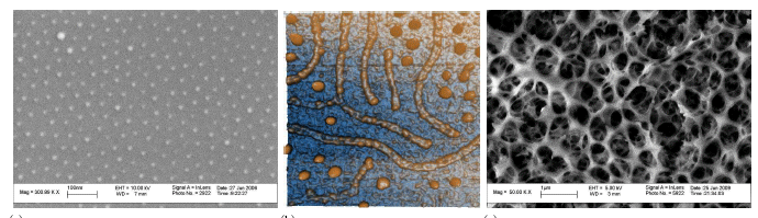
Block Copolymer Lithography (a) SEM image of a quasi-ordered array of 15 nm gold nanoparticles on glass produced by BCPL. b) AFM image of Ni nanoprints formed by BCPL. c) SEM image of Rh oxide fashioned into an inverse opal structure via BCPL.
Chemical Vapor Deposition
Thin films and coatings will also play a part in advanced nanoscale structures, in particular metal oxides supports for catalysis and plasmon assisted charge transfer. Devices derived from thin films are ubiquitous in electronics, phontonics, and active materials, and metal organic chemical vapor deposition (MOCVD) is widely considered to produce films of the highest quality. Simply stated, MOCVD involves exposing a heated substrate to flow of vaporized precursors that react with the substrate and deposit a film. The process variables include the precursor flux, substrate temperature, chamber pressure, and background pressure. In the MOCVD reactor system developed at Caltech, we are able to control the relative amount of each component of the precursor flux in real-time. This allow us to create complex multi-component films, and more recently, we have extended this capability to created arbitrary heterostructures, e.g. compositionally graded films, Figure 5. The immediate impact of this technology is to create a ferroelectric with a high dielectric constant that is constant over a wide temperature range. I believe that this method of control can also be applied to creating third generation photovoltaics, e.g. CIGS. In addition, I am interested in studying the mechanical stress in these structures, via coherent gradient sensing, and how it relates to the microstructure .
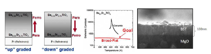
Advanced MOCVD Compositionally graded BaxSr(1-x)TiO3 films by MOCVD. "up" and "down" graded films; desired dielectric response with temperature; SEM cross section of a BST film on MgO produced in our lab. (left to right, respectively).